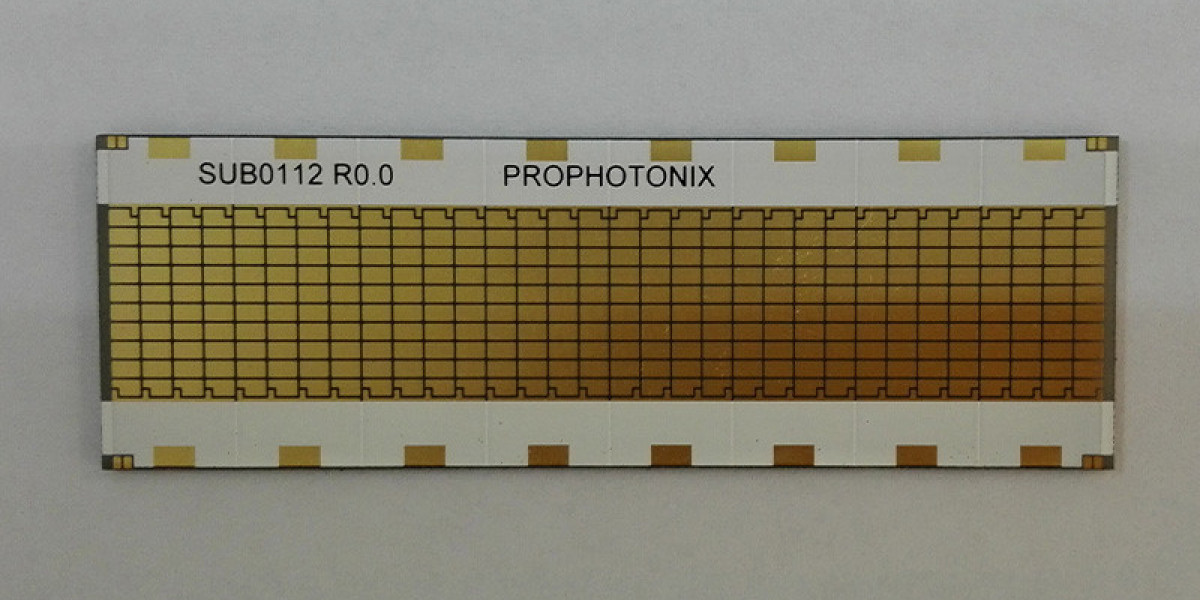
The metallized ceramic substrate is a type of circuit board with a thermal expansion coefficient similar to that of semiconductors and high heat resistance. It is ideal for products with high heat generation, such as high-brightness LEDs and solar energy devices, and its excellent weather resistance makes it particularly suited for harsh outdoor environments. With features like being lead-free, non-toxic, and chemically stable, it poses no harm to the environment, which is why it is increasingly gaining acceptance.
Due to different technology, the ceramic substrate is mainly divided into DPC (Direct Plated Copper), DBC (Direct Bonded Copper), AMB (Active Metal Brazing), and Thick film.
Below is the introduction for each of the processes and the advantages, disadvantages of each process.
DPC (Direct Plated Copper)
DPC is recent development in the field of Ceramic Substrate PCBs and was the breakthrough that made ceramics much more viable to designers. DPC involves vacuum sputtering under high temperature and pressure conditions to plate the copper to the substrate. The addition of a thin film titanium (Ti) layer acts as a bonding interface between the copper and ceramic layers. DPC can only deposit very thin copper film onto the ceramic substrate, need to combine traditional plating process to reach thick copper thickness requirement.
Advantages:
- In terms of shape processing, DPC ceramic plate needs to be cut by laser, the traditional drilling and milling machine, and punch machine can not be accurately processed, so the combined force and line width are also finer.
- The crystal performance of the metal is good;
- The flatness is good;
- The trace is not easy to fall off;
- The trace position is more accurate, the line distance is smaller, reliable, and stable, can be through the hole and other advantages.
Disadvantages:
It can only make a thin plate (thickness < 300μm), and its cost is high, the output value is limited, resulting in frequent shipment time can not be on time.
DBC (Direct Bonded Copper)
With DBC the copper is bonded to the Ceramic substrates on one or both sides using a high-temperature oxidation process. It offers options of heavy copper thickness above 100μm. The copper and substrate are heated in an atmosphere of nitrogen containing about 30ppm of oxygen; under these conditions, a copper-oxygen eutectic forms which bonds successfully both to copper and the oxides used as substrates. With DBC the copper layers can then be etched using standard PCB technology to form required circuit.
Advantages:
- The copper layer is thick;
- The processing is fast;
- The price is cheap;
- Can make multilayer;
- Suitable for large area consumption;
- High thermal conductivity;
- High adhesion strength;
- Excellent soft brazing;
- Excellent electrical insulation
Disadvantages:
- Can not pass through the hole;
- Poor accuracy;
- Low flatness (surface roughness);
- Suitable for the device in the large distance of the product, can not be done in the precise occupation.
AMB (Active Metal Brazing)
Active Metal Brazing(AMB) forms the substrates without metallization. Under a high temperature vacuum the copper is joined (brazed) direct to the ceramic base. This offers a high reliability substrate with unique heat dissipation. The brazing technology also enables copper weights of up to 800μm on thin ceramic substrates. These heavy copper materials make AMB ideal for power electronics.
Advantages:
The combination is achieved by the chemical reaction between ceramic and active metal solder paste at high temperatures, so its bonding strength is higher and reliability is better.
Disadvantages:
The reliability of the AMB process depends largely on the composition of active filler metal, brazing process, brazing layer structure, and many other key factors.
Thick film
Thick film technology is a process of printing patterns directly on a ceramic substrate and then sintering it directly.
Advantages:
- The bonding force with ceramic is much greater than that of the DPC process;
- It is direct printing of graphics, no etching, and copper plating process, so the cost will be lower;
- It is a one-time forming, so the flatness is smoother than that of the DPC.
Disadvantages:
Because the thick film process is printed, it is generally not too thick. Due to different product requirements, different materials have a certain impact on the conductivity of the film.
In conclusion, it is hard to say which process is best, it depends on the customer’s application and usage, customer could choose each of the processes according to their requirements.
Should you have more interests, pls feel free to contact us at any time. If you want to know more about the ceramic PCB, you can enter below website: https://hitechcircuits.com/pcb-products/ceramic-pcb/